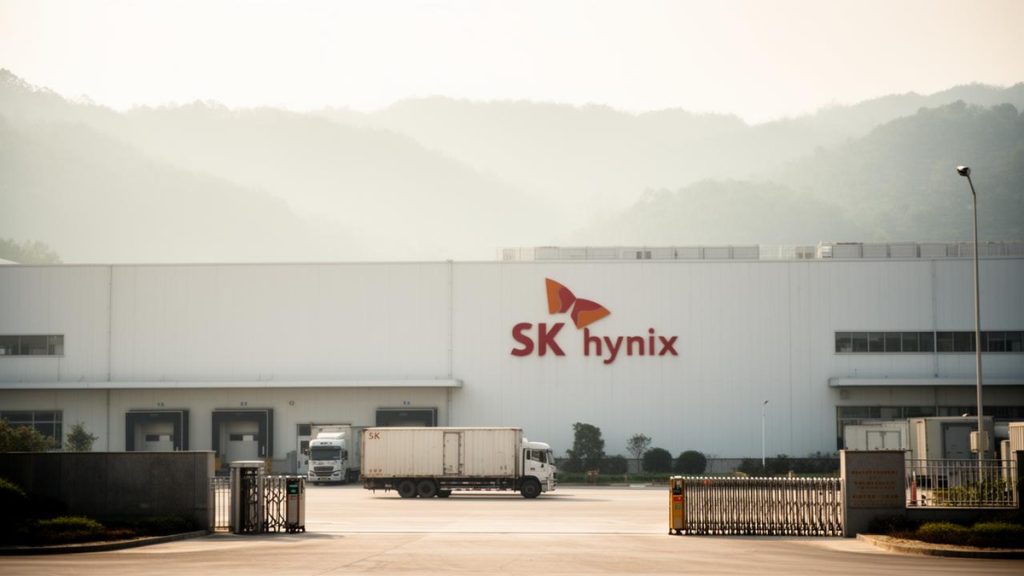
South Korean memory chip titan SK Hynix is mulling a major capital restructuring of its Chinese assets. According to a Bloomberg report citing sources familiar with the matter, the company is considering bringing in outside investors for its large-scale semiconductor packaging and testing base in Chongqing. If the transaction involves selling a partial stake, the facility’s overall valuation could reach approximately $30 billion. The development is being interpreted by observers as a key step for SK Hynix to optimize its China business footprint against the backdrop of a reshaping global semiconductor supply chain.
SK Hynix has reportedly begun engaging with potential advisors to help evaluate various strategic options for the Chongqing plant. Sources indicated that the options under discussion include introducing strategic investors to accelerate the independent development of the business. The pool of potential buyers is primarily China-based, encompassing Chinese investment funds and related enterprises along the semiconductor industry chain. Should a deal materialize, SK Hynix is not expected to exit entirely but would likely retain a minority stake in the asset to maintain its strategic presence in the Chinese market.
However, the sources stressed that the evaluation and discussions are at a very preliminary stage, and there remains considerable uncertainty as to whether any transaction will ultimately proceed. A representative for SK Hynix declined to comment on the matter as of press time.
A Packaging Powerhouse Two Decades in the Making
The Chongqing plant holds a special position in SK Hynix’s global production map. According to information disclosed on SK Hynix’s official website, the company has been in the Chinese market for over 20 years. Its early landmark move was signing an agreement in Wuxi, an eastern Chinese city, to build its first large-scale overseas wafer fabrication plant. The Chongqing facility, by contrast, is positioned as a large-scale semiconductor packaging and testing base, primarily handling the back-end production of SK Hynix’s NAND flash memory. It has played a crucial supporting role in driving the company’s global NAND flash output growth.
Even as it evaluates bringing investors into the Chongqing plant, SK Hynix’s expansion pace in South Korea shows no signs of slowing—in fact, it appears to be accelerating. Just this Friday, the company formally announced an unprecedented domestic investment plan, committing 54 trillion won (approximately $38 billion) to expand its chip manufacturing facilities in South Korea.
This massive investment will focus on two core areas: building an advanced DRAM fabrication plant in Yongin, Gyeonggi Province, and constructing a brand-new NAND flash production facility in Cheongju, North Chungcheong Province. SK Hynix explicitly stated that the move aims to fully address the explosive growth in memory chip demand driven by the artificial intelligence era.
Strategic Pivot Toward Domestic Advanced Capacity
This series of moves by SK Hynix reflects its deep strategic logic amid the seismic shifts in the global semiconductor landscape. As a core supplier of High Bandwidth Memory (HBM) to Nvidia, SK Hynix sits at the epicenter of the AI computing storm. HBM, an indispensable key component in AI servers, is seeing its demand swell dramatically with the iteration of large language models. To solidify and expand its leadership in this high-margin segment, SK Hynix must concentrate its largest capital expenditures and most advanced technological resources in South Korea.
Market analysts note that through the massive investments in Yongin and Cheongju, SK Hynix aims to further widen the technological gap with competitors in cutting-edge DRAM and NAND flash. The potential plan to seek strategic investors for the Chongqing plant, meanwhile, may signal that the company hopes to moderately adjust its asset-heavy holding structure without relinquishing the benefits of the Chinese market. By bringing in Chinese strategic investors, SK Hynix could not only recoup some capital to support its hefty spending but also leverage local capital to give the Chongqing packaging and testing business more flexible room to develop in an increasingly complex market environment.
In terms of asset attributes, packaging and testing belong to the back-end segment of the semiconductor industry chain, carrying lower technological sensitivity and added value compared to front-end wafer fabrication. This may be one reason why SK Hynix is willing to take the lead in adjusting the equity structure in this segment. Currently, there is no indication that SK Hynix plans similar moves for its front-end wafer fabrication plant in Wuxi.
A Balancing Act Amid Global Supply Chain Restructuring
This asset evaluation plan comes at a critical juncture when major global economies are placing increasing emphasis on the localization and diversification of semiconductor supply chains. For a South Korean chip giant with substantial manufacturing assets in China, striking a balance between complying with international trade rules, responding to domestic strategic needs, and maintaining market share in the world’s largest semiconductor consumer market has become an imperative question.
The news that SK Hynix intends to introduce investors for its Chongqing plant suggests the chip titan is attempting a more pragmatic and flexible strategy for the Chinese market. If the transaction ultimately lands, it will not only reshape SK Hynix’s asset map in China but could also provide a new capital restructuring template for other overseas semiconductor firms with heavy assets in the country.
Going forward, as the evaluation work deepens, the identity of potential buyers, the specific equity sale ratio, and the transaction timeline will become focal points for the market. Meanwhile, the construction progress of SK Hynix’s new plants in Yongin and Cheongju will directly determine its standing in the next round of the AI memory chip race.